Loading...
← Back to Prompts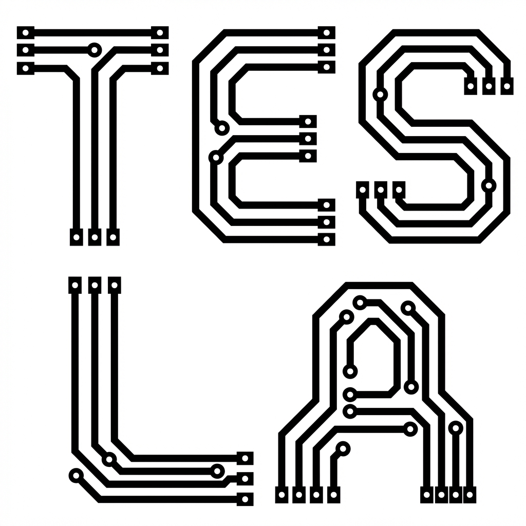
Word Constructed from PCB Traces
Nano Banana Procreativeartstyle+4 more
Nano Banana ProcreativeartstylelogodesignAnime StylePhotorealistic3D Art
Works With
Nano Banana Pro
May 14, 2026
0Views0Likes0Shares
Prompt
Anchor: The word "{argument name="word to construct" default="Tesla"}" :: constructed entirely from printed circuit board traces, where each letterform is a functional-looking PCB layout — solder pads as terminals, vias as joints, trace paths forming the strokes ::4 Morphology: Technical PCB illustration. Letter strokes are traces of varying widths. Circular vias punctuate stroke junctions. Solder pad rectangles anchor stroke terminals. The letters read as living circuit diagrams. Monochrome technical vector ::3 Material Physics: Jet black trace lines on white substrate, exposed copper-pad circles with concentric detail rings, uniform stroke weight with deliberate corner chamfers (45°) ::3 Illumination: Flat technical illustration lighting, no depth, pure 2D schematic clarity ::2 Render Stack: Electronics schematic aesthetic, hardware documentation style, Gerber file visual output ::1 Negative: [Silhouette shapes, actual electronic components, chip illustrations, realistic PCB green color, perspective, photographic textures, solder reflections] ::-1
What This Prompt Creates
Anchor: The word "{argument name="word to construct" default="Tesla"}" :: constructed entirely from printed circuit board traces, where each letterform is a functional-looking PCB layout — solder pads
Best Used For
nano_banana